
SK Hynix, a semiconductor leader, has made a significant stride in the NAND Flash industry by revealing a prototype of its pioneering 321-layer 4D NAND at the Flash Memory Summit (FMS) 2023 held from August 8-10 in Santa Clara. This unveiling marks a remarkable achievement as SK Hynix becomes the first company to present progress on developing NAND technology with over 300 layers.
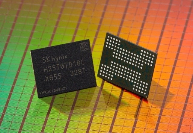 During the presentation, SK Hynix showcased the development journey of its cutting-edge 321-layer 1Tb Triple Level Cell (TLC) 4D NAND Flash. The technological advancement allows for an impressive 59 percent boost in productivity compared to the previous 238-layer 512Gb generation. This achievement is attributed to the innovative stacking of more cells and the incorporation of a larger storage capacity within a single chip. The expansion in storage capacity paves the way for enhanced data processing capabilities and greater efficiency.
Building on the success of its currently mass-produced 238-layer NAND, SK Hynix’s seamless progression to the 321-layer technology exemplifies the company’s prowess in overcoming stacking limitations. As a result, the firm is on track to initiate mass production of the 321-layer NAND from the first half of 2025.
Jungdal Choi, the Head of NAND Development at SK Hynix, emphasized the strategic significance of this milestone during a keynote speech at the FMS. Choi highlighted that the ongoing development of the 321-layer product, the fifth generation of 4D NAND, reinforces SK Hynix’s technological leadership in the NAND landscape. He stated, “With the timely introduction of high-performance and high-capacity NAND, we will strive to meet the requirements of the AI era and continue to lead innovation.”
As the demand for high-performance and high-capacity memory products continues to surge, driven by the rapid growth of the generative AI market, SK Hynix has responded by introducing next-generation NAND solutions tailored to address these evolving needs.
Among the unveiled offerings are enterprise Solid-State Drives (SSDs) adopting the PCIe Gen5 interface and UFS 4.0. These products are expected to deliver better performance, effectively catering to the requirements of customers in search of top-tier capabilities.
Furthermore, SK Hynix has announced its development efforts for the next-generation PCIe Gen6 and UFS 5.0. These initiatives are underpinned by the advancements in technology gained through the development of its latest NAND solutions, reinforcing the company’s commitment to driving industry trends and maintaining its leadership position.
SK Hynix’s strides in NAND technology, particularly the groundbreaking 321-layer 4D NAND, not only signify a significant leap forward in data storage capabilities but also position the company at the forefront of innovation in the semiconductor landscape. With its forward-looking approach, SK Hynix is poised to play a pivotal role in shaping the AI-driven future of data processing and storage.