
Samsung Electronics, the global leader in semiconductor technology, has started production of its 3-nanometer (nm) process node applying Gate-All-Around (GAA) transistor architecture — beating TSMC.
 TSMC, the world’s largest contract chip manufacturer, said it will begin mass production of 3nm chips in the second half of the year.
Samsung, the world’s largest memory chip maker and second largest foundry player, has said its 2nm process node was in the early stages of development, with mass production planned for 2025.
Samsung’s GAA technology called Multi-Bridge-Channel FET (MBCFET), implemented for the first time ever, defies the performance limitations of FinFET, improving power efficiency by reducing the supply voltage level, while enhancing performance by increasing drive current capability.
Samsung is starting the first application of the nanosheet transistor with semiconductor chips for high performance, low power computing applications and plans to expand to mobile processors, Samsung said in a news statement.
The Capex of Samsung during the first quarter of 2022 stood at KRW 7.9 trillion, including KRW 6.7 trillion spent on semiconductors and KRW 0.7 trillion on displays.
 Samsung earlier said spending on memory was concentrated on infrastructure at P3 and on process migrations at fabs in Hwaseong, Pyeongtaek and Xi’an. Samsung’s foundry investments were focused on developing and establishing the production capacity of under 5-nanometer advanced processes.
“Samsung has grown rapidly as we continue to demonstrate leadership in applying next-generation technologies to manufacturing, such as the foundry industry’s first High-K Metal Gate, FinFET, as well as EUV. We seek to continue this leadership with the world’s first 3nm process with the MBCFET,” said Dr. Siyoung Choi, President and Head of Foundry Business at Samsung Electronics.
Samsung’s technology utilizes nanosheets with wider channels, which allow higher performance and greater energy efficiency compared to GAA technologies using nanowires with narrower channels. Utilizing the 3nm GAA technology, Samsung will be able to adjust the channel width of the nanosheet in order to optimize power usage and performance to meet various customer needs.
The design flexibility of GAA is advantageous for Design Technology Co-Optimization (DTCO), which helps boost Power, Performance, Area (PPA) benefits.
Samsung said compared to 5nm process, the first-generation 3nm process can reduce power consumption by up to 45 percent, improve performance by 23 percent, and reduce area by 16 percent compared to 5nm, while the second-generation 3nm process is to reduce power consumption by up to 50 percent, improve performance by 30 percent, and reduce area by 35 percent.
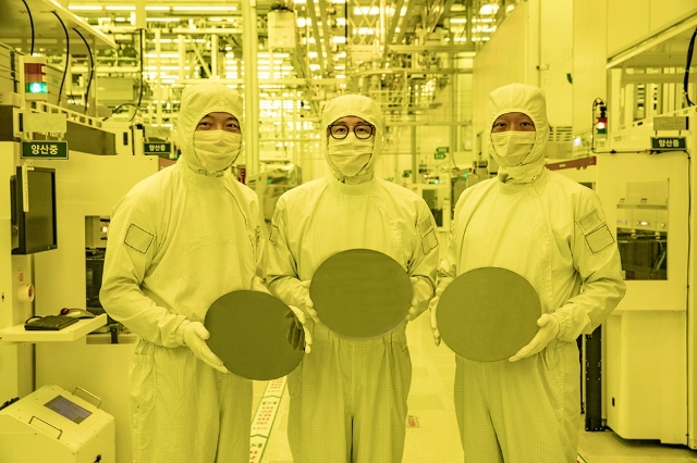
Image: (From left) Michael Jeong, Corporate Vice President; Ja-Hum Ku, Corporate Executive Vice President; and Sang Bom Kang, Corporate Vice President at Samsung Foundry Business are holding up 3nm wafers at the production line of Samsung Electronics Hwaseong Campus.


